東京大学 情報理工学系研究科 電子情報学専攻 2023年度 専門 第2問
Author
Description
Let us design a circuit that adds a 4-bit signed integer \(A(A_{3:0})\) and a 3-bit signed integer \(B(B_{2:0})\) and outputs a 4-bit signed integer \(Y(Y_{3:0})\). Two's complement is used to represent signed integers. Let \(A_3,B_2\), and \(Y_3\) be the MSB(Most Significant Bit). Answer the following questions.
(1) Show the ranges of possible values of \(A\) and \(B\) in decimal notation.
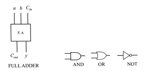
(2) Show the truth table for the 1-bit full adder shown on the left side of the figure below. Let \(a\) and \(b\) be operands, \(C_{in}\) be the input carry, \(y\) be the output, and \(C_{out}\) be the output carry.
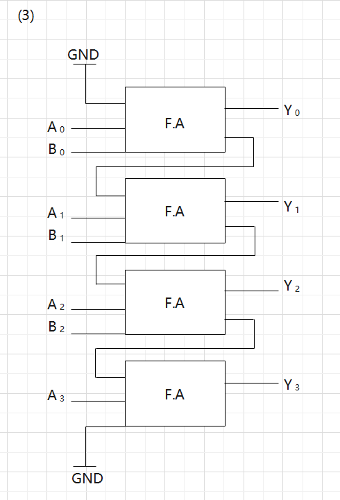
(3) Show the circuit that computes \(Y = A + B\) by combining the full-adder symbols used in (2). Also, show the input/output signal lines. You can use supply voltage V\(_{\text{DD}}\) and ground GND if necessary.
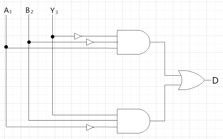
(4) Let us add an overflow detection function to the circuit in (3). The additional circuit takes a 1-bit signal \(D\) as output, with \(D = 1\) when an overflow occurs and \(D = 0\) otherwise. Show the truth table of the circuit to output \(D\) by using necessary signals. Also, show the circuit that generates \(D\) by combining necessary signals and gates from \(A_{3:0}, B_{2:0}, C_{3:0}\), AND, OR, and NOT shown on the right side of the figure below. The number of gates and inputs can be increased, but the circuit should be simple.
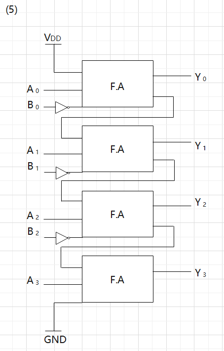
(5) Let us design a circuit to compute \(Y = A - B\) instead of adding \(A\) and \(B\). Show the circuit by combining full-adders, AND, OR, and NOT gates. Similar to (3), input/output signal lines should also be shown. You can use V\(_{\text{DD}}\) and GND if necessary.
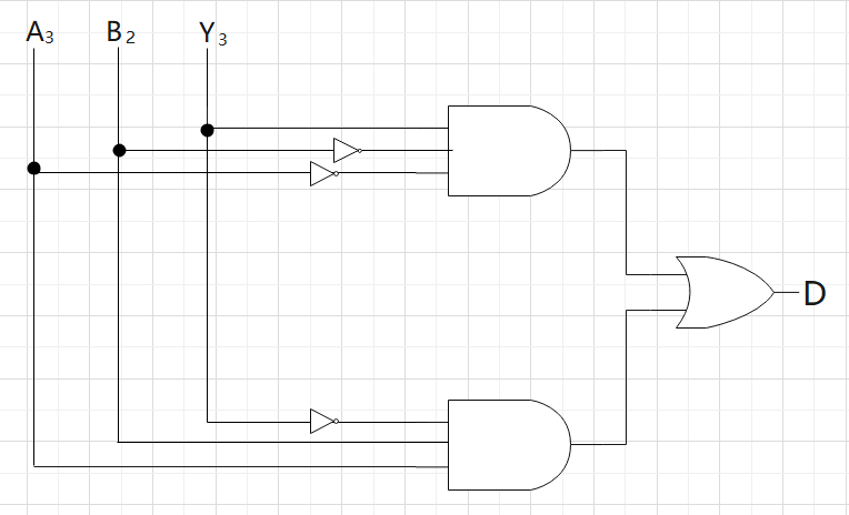
(6) Let us add an overflow detection function to the circuit in (5) as in (4). The additional circuit takes a 1-bit signal \(D\) as output, with \(D = 1\) when an overflow occurs and \(D = 0\) otherwise. Show the truth table of the circuit to output \(D\) by using necessary signals. Also, show the circuit that genrates \(D\) by combining necessary signals and gates from \(A_{3:0},B_{2:0},Y_{3:0}\), AND, OR, and NOT shown on the right side of the figure below. The number of gates and inputs can be increased, but the circuit should be simple.
Kai
(1)
\(A:[-8,7],\quad B:[-4,3]\)
(2)
| \(a\) | \(b\) | \(C_{in}\) | \(y\) | \(C_{out}\) |
|---|---|---|---|---|
| 0 | 0 | 0 | 0 | 0 |
| 0 | 0 | 1 | 1 | 0 |
| 0 | 1 | 0 | 1 | 0 |
| 0 | 1 | 1 | 0 | 1 |
| 1 | 0 | 0 | 1 | 0 |
| 1 | 0 | 1 | 0 | 1 |
| 1 | 1 | 0 | 0 | 1 |
| 1 | 1 | 1 | 1 | 1 |
(3)
(4)
| \(A_3\) | \(B_2\) | \(Y_3\) | D |
|---|---|---|---|
| 0 | 0 | 0 | 0 |
| 0 | 0 | 1 | 1 |
| 0 | 1 | 0 | 0 |
| 0 | 1 | 1 | 0 |
| 1 | 0 | 0 | 0 |
| 1 | 0 | 1 | 0 |
| 1 | 1 | 0 | 1 |
| 1 | 1 | 1 | 0 |
(5)
(6)
| \(A_3\) | \(B_2\) | \(Y_3\) | D |
|---|---|---|---|
| 0 | 0 | 0 | 0 |
| 0 | 0 | 1 | 0 |
| 0 | 1 | 0 | 0 |
| 0 | 1 | 1 | 1 |
| 1 | 0 | 0 | 1 |
| 1 | 0 | 1 | 0 |
| 1 | 1 | 0 | 0 |
| 1 | 1 | 1 | 0 |