東京大学 情報理工学系研究科 電子情報学専攻 2020年度 専門 第2問
Author
Description
Let us design a circuit that obtains a 4-bit signed integer \(Y_{3..0}\) by calculating 4-bit additon/subtraction of a 4-bit signed integer \(A_{3..0}\) and a 2-bit signed integer \(B_{1,0}\). The integers \(A,B\) and \(Y\) are expressed in two's complement. The types of logic gates that you can use arc NOT, AND , OR ,and , XOR , cach of which is equipped with as many inputs as the design requires. Answer the following questions.
(1) Show the maximum and minimum values of \(A\) and \(B\) in decimal form.
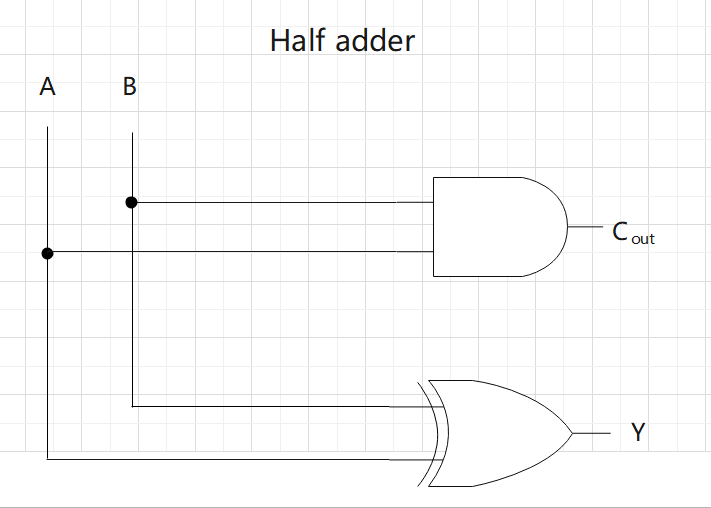
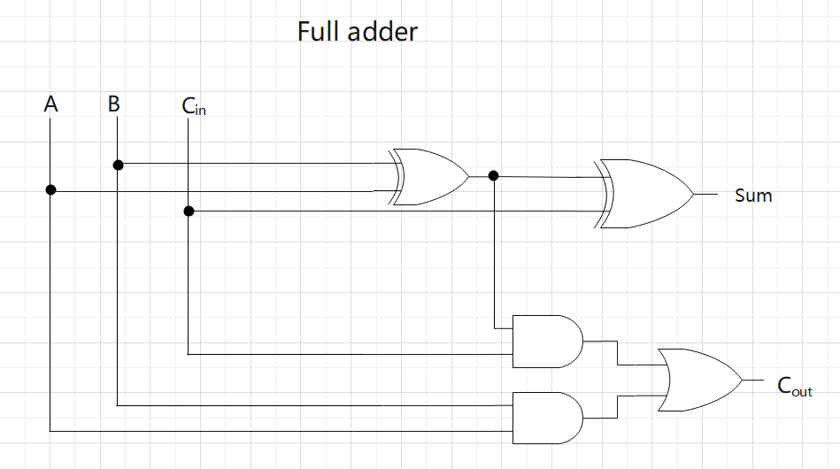
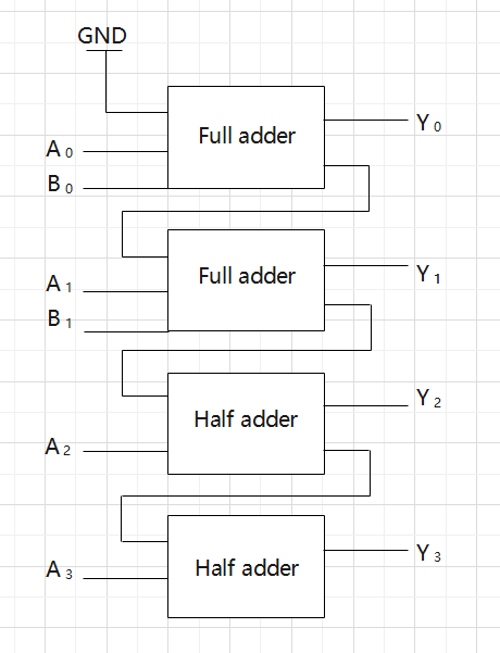
(2) Show a circuit that calculates \(A + B\) to obtain \(Y\) by combining logic gates. Organize the adder as a ripple carry adder. You can use signals from \(A_{3..0},B_{1,0}\), supply voltage \(V_{DD}\), and grounding voltage GND as inputs, The output should be \(Y_{3..0}\). To simplify the diagram, use the "half-adder" blocks and the "full-adder" blocks after showing gate-level designs of both blocks.
(3) Consider adding an overflow detection mechanism to the circuit designed in (2). Show the overflow detection circuit by combining the logic gates. You can use signals from \(A_{3..0},B_{1,0}\) and \(Y_{3..0}\) as inputs. The output should be a 1-bit signal named \(D\); it should be '1' when the overflow occured, or '0' otherwise.
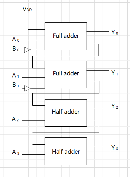
(4) Show a circuit that calculates \(A - B\) to obtain \(Y\) by combining logic gates. Organize the adder as a ripple carry adder. You can use signals from \(A_{3..0},B_{1,0},V_{DD}\) and GND as inputs. The output should be \(Y_{3..0}\). Use the "half-adder" blocks and the "full-adder" blocks in (2).
(5) Show all the input patterns that cause overflows for the calculation designed in (4).
Kai
(1)
(2)
(3)
(2) で設計した回路がオーバーフローするとき、\(A_3C_2=1\) となる。 また、(2) の回路は以下の論理式を満たす。
これらの式を代入して
よって求めるオーバーフロー検知機構の回路は次の通り。

(4)
(5)
1ビットの信号 \(D\) でオーバフローかどうかを出力し、オーバフロー発生時に \(1\)、そうでないときに \(0\) を出力するとする。
(3) と同じように考え、\(D = 1\) となるのは以下の論理式を満たす場合である。
これを解いて
以上からオーバフローが発生する入力パターンは以下の通り。ただし、 \(*\) は \(0\) でも \(1\) でも良い。
| \(A_0\) | \(A_1\) | \(A_2\) | \(A_3\) | \(B_0\) | \(B_1\) |
|---|---|---|---|---|---|
| 1 | 1 | 1 | 1 | * | * |
| 1 | * | 1 | 1 | * | 0 |
| * | 1 | 1 | 1 | 0 | * |
| 0 | 0 | 1 | 1 | 0 | 0 |
| * | 1 | 1 | 1 | * | 0 |