東京大学 情報理工学系研究科 電子情報学専攻 2022年8月実施 専門 第2問
Author
Description
Let us design a circuit that adds a 4-bit signed integer and a 3-bit signed integer and outputs a 4-bit signed integer . Two's complement is used to represent signed integers. Let , and be the MSB(Most Significant Bit). Answer the following questions.
(1) Show the ranges of possible values of and in decimal notation.
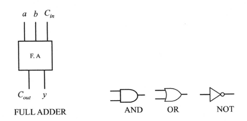
(2) Show the truth table for the 1-bit full adder shown on the left side of the figure below. Let and be operands, be the input carry, be the output, and be the output carry.
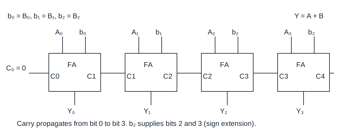
(3) Show the circuit that computes by combining the full-adder symbols used in (2). Also, show the input/output signal lines. You can use supply voltage V and ground GND if necessary.
(4) Let us add an overflow detection function to the circuit in (3). The additional circuit takes a 1-bit signal as output, with when an overflow occurs and otherwise. Show the truth table of the circuit to output by using necessary signals. Also, show the circuit that generates by combining necessary signals and gates from , AND, OR, and NOT shown on the right side of the figure below. The number of gates and inputs can be increased, but the circuit should be simple.
(5) Let us design a circuit to compute instead of adding and . Show the circuit by combining full-adders, AND, OR, and NOT gates. Similar to (3), input/output signal lines should also be shown. You can use V and GND if necessary.
(6) Let us add an overflow detection function to the circuit in (5) as in (4). The additional circuit takes a 1-bit signal as output, with when an overflow occurs and otherwise. Show the truth table of the circuit to output by using necessary signals. Also, show the circuit that genrates by combining necessary signals and gates from , AND, OR, and NOT shown on the right side of the figure below. The number of gates and inputs can be increased, but the circuit should be simple.
题目描述
设计一个把 位有符号整数 与 位有符号整数 相加,并输出 位有符号整数 的电路。有符号数采用二进制补码表示, 分别为最高有效位。题目所用全加器和逻辑门符号见上图。
(1) 用十进制写出 、 的取值范围。
(2) 写出上图左侧一位全加器的真值表,其中 为操作数, 为输入进位, 为和位输出, 为输出进位。
(3) 组合 (2) 的全加器符号,画出计算 的电路,并标明输入、输出信号线;必要时可使用电源 和地 GND。
(4) 为 (3) 增加溢出检测功能,输出一位信号 :溢出时 ,否则 。使用必要信号写出 的真值表;再利用 中所需信号以及上图右侧所示的 AND、OR、NOT 门画出生成 的电路。门和门输入数可以增加,但电路应尽量简单。
(5) 改为设计计算 的电路,组合全加器以及 AND、OR、NOT 门,并像 (3) 一样标明输入、输出信号线;必要时可使用 和 GND。
(6) 像 (4) 一样为 (5) 增加一位溢出信号 。使用必要信号写出真值表,并利用 中所需信号以及 AND、OR、NOT 门画出尽量简单的 生成电路;门和输入数可以增加。
Kai
(1)
(2)
| 0 | 0 | 0 | 0 | 0 |
| 0 | 0 | 1 | 1 | 0 |
| 0 | 1 | 0 | 1 | 0 |
| 0 | 1 | 1 | 0 | 1 |
| 1 | 0 | 0 | 1 | 0 |
| 1 | 0 | 1 | 0 | 1 |
| 1 | 1 | 0 | 0 | 1 |
| 1 | 1 | 1 | 1 | 1 |
(3)
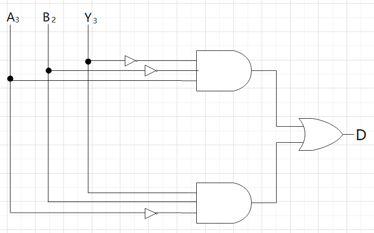
(4)
| D | |||
|---|---|---|---|
| 0 | 0 | 0 | 0 |
| 0 | 0 | 1 | 1 |
| 0 | 1 | 0 | 0 |
| 0 | 1 | 1 | 0 |
| 1 | 0 | 0 | 0 |
| 1 | 0 | 1 | 0 |
| 1 | 1 | 0 | 1 |
| 1 | 1 | 1 | 0 |
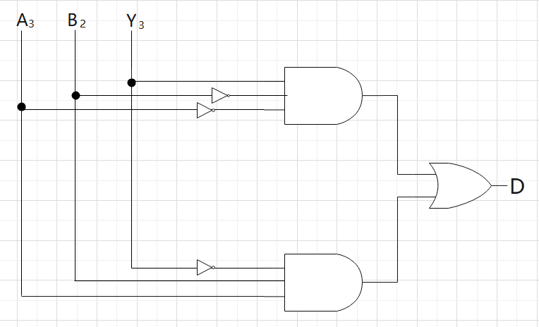
(5)
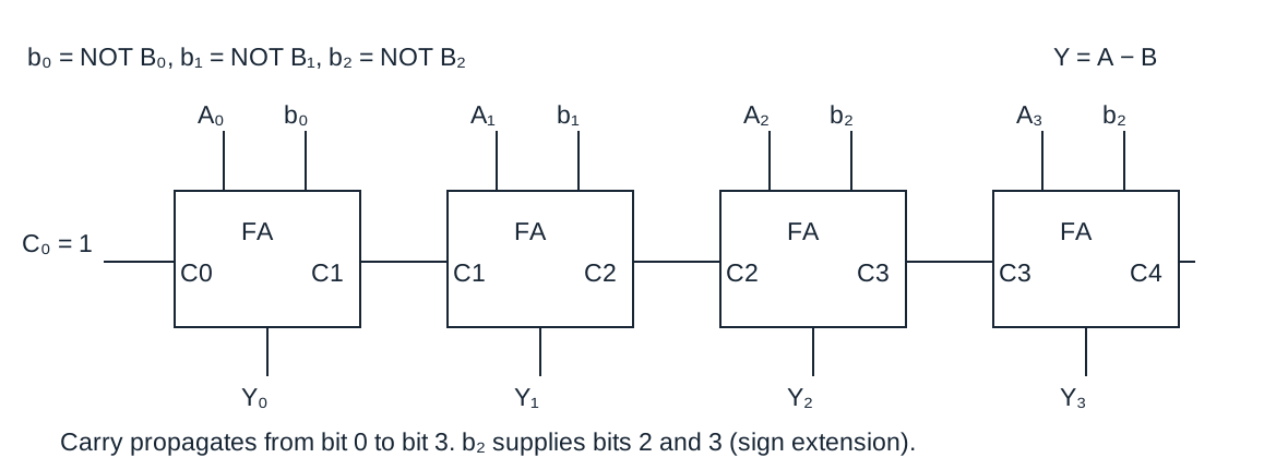
(6)
| D | |||
|---|---|---|---|
| 0 | 0 | 0 | 0 |
| 0 | 0 | 1 | 0 |
| 0 | 1 | 0 | 0 |
| 0 | 1 | 1 | 1 |
| 1 | 0 | 0 | 1 |
| 1 | 0 | 1 | 0 |
| 1 | 1 | 0 | 0 |
| 1 | 1 | 1 | 0 |