東京大学 情報理工学系研究科 電子情報学専攻 2016年8月実施 専門 第2問
Author
Description
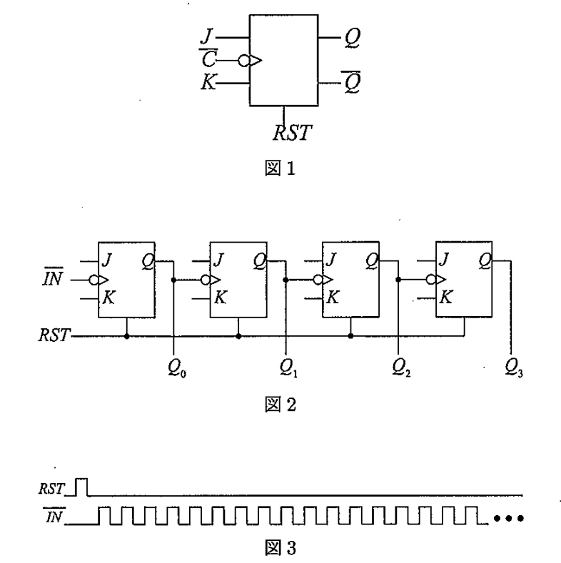
Let us consider a falling-edge-triggered JK flip-flop as shown in Fig.1. This JK flip-flop is reset to when . Answer the following questions.
(1) Let us assume a 4-bit counter as shown in Fig.2, and the input signals shown in Fig.3 are given to the counter. Show a time chart of the outputs . Here, let us assume that all the and terminals are connected to 1, and the delay of each JK flip-flop, , cannot be neglected.
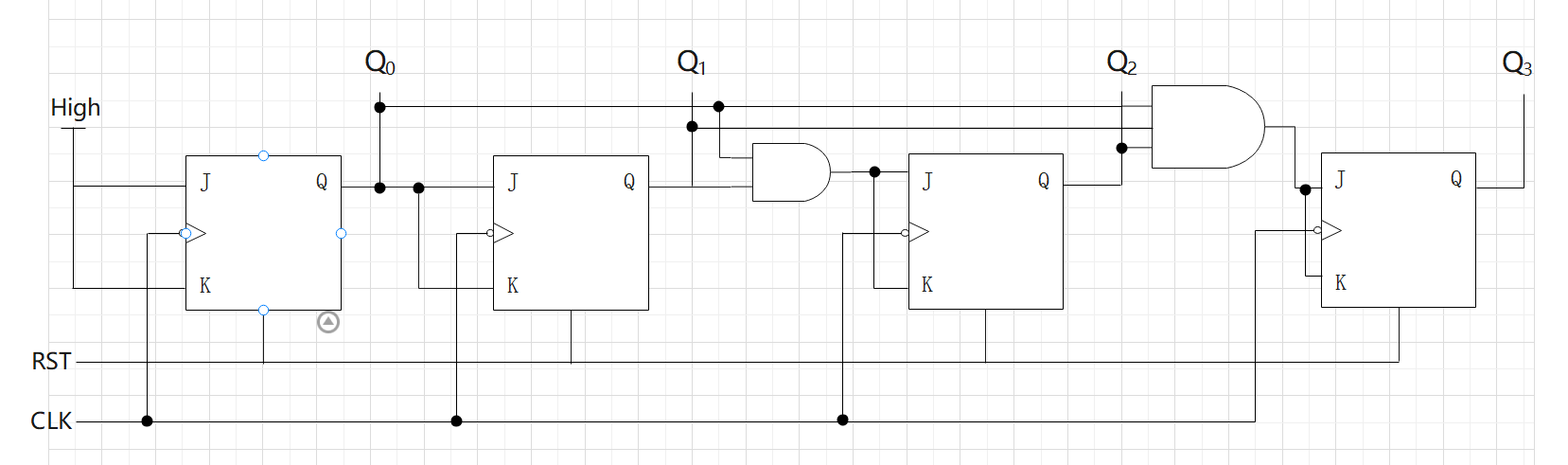
(2) Modify the circuit in Fig.2 so that the outputs change simultaneously, and show its schematic. (Such a circuit is called a parallel counter or a synchronous counter.)
(3) Let us design a parallel decimal counter. A decimal counter is a circuit that starts counting from () = (0000) up to () = (1001) and then returns to () = (0000) in the next state. Show a state transition diagram and a Karnaugh map of the counter.
(4) Show a schematic of a parallel decimal counter by using the results in (3).
(5) Modify the circuit in (2) to an up/down counter and show its schematic. An up/down counter is a counter whose operation mode can be changed either to count-up or count-down by a control signal .
题目描述
考虑图 1 所示下降沿触发 JK 触发器。当 时,触发器复位为 。图 2、图 3 及所用符号均见上图,回答下列问题。
(1) 对图 2 的 位计数器输入图 3 所示信号,画出输出 ~ 的时序图。假设所有 、 端均接 ,且每个 JK 触发器的延迟 不可忽略。
(2) 修改图 2 的电路,使 ~ 同时变化,并画出电路图。这种电路称为并行计数器或同步计数器。
(3) 设计一个并行十进制计数器:从 计数到 ,下一状态返回 。画出其状态转移图和卡诺图。
(4) 利用 (3) 的结果,画出并行十进制计数器的电路图。
(5) 把 (2) 的电路改造成加/减计数器并画出电路图。该计数器通过控制信号 在向上计数和向下计数两种模式间切换。
Kai
(1)
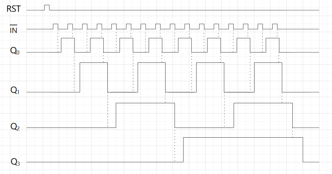
Let be the time of the -th falling input edge after reset. For , toggles precisely when is a multiple of , at time . The clock period is assumed long enough for the ripple to settle.
(2)
(3)
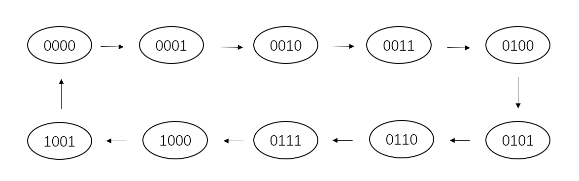
| 0 | 0 | 0 | 0 | 0 | 0 | 0 | 1 |
| 0 | 0 | 0 | 1 | 0 | 0 | 1 | 0 |
| 0 | 0 | 1 | 0 | 0 | 0 | 1 | 1 |
| 0 | 0 | 1 | 1 | 0 | 1 | 0 | 0 |
| 0 | 1 | 0 | 0 | 0 | 1 | 0 | 1 |
| 0 | 1 | 0 | 1 | 0 | 1 | 1 | 0 |
| 0 | 1 | 1 | 0 | 0 | 1 | 1 | 1 |
| 0 | 1 | 1 | 1 | 1 | 0 | 0 | 0 |
| 1 | 0 | 0 | 0 | 1 | 0 | 0 | 1 |
| 1 | 0 | 0 | 1 | 0 | 0 | 0 | 0 |
The unused states 1010–1111 are don’t-cares. Rows and columns are in Gray-code order.
| \ | 00 | 01 | 11 | 10 |
|---|---|---|---|---|
| 00 | 1 | 0 | 0 | 1 |
| 01 | 1 | 0 | 0 | 1 |
| 11 | x | x | x | x |
| 10 | 1 | 0 | x | x |
| \ | 00 | 01 | 11 | 10 |
|---|---|---|---|---|
| 00 | 0 | 1 | 0 | 1 |
| 01 | 0 | 1 | 0 | 1 |
| 11 | x | x | x | x |
| 10 | 0 | 0 | x | x |
| \ | 00 | 01 | 11 | 10 |
|---|---|---|---|---|
| 00 | 0 | 0 | 1 | 0 |
| 01 | 1 | 1 | 0 | 1 |
| 11 | x | x | x | x |
| 10 | 0 | 0 | x | x |
| \ | 00 | 01 | 11 | 10 |
|---|---|---|---|---|
| 00 | 0 | 0 | 0 | 0 |
| 01 | 0 | 0 | 1 | 0 |
| 11 | x | x | x | x |
| 10 | 1 | 0 | x | x |
(4)
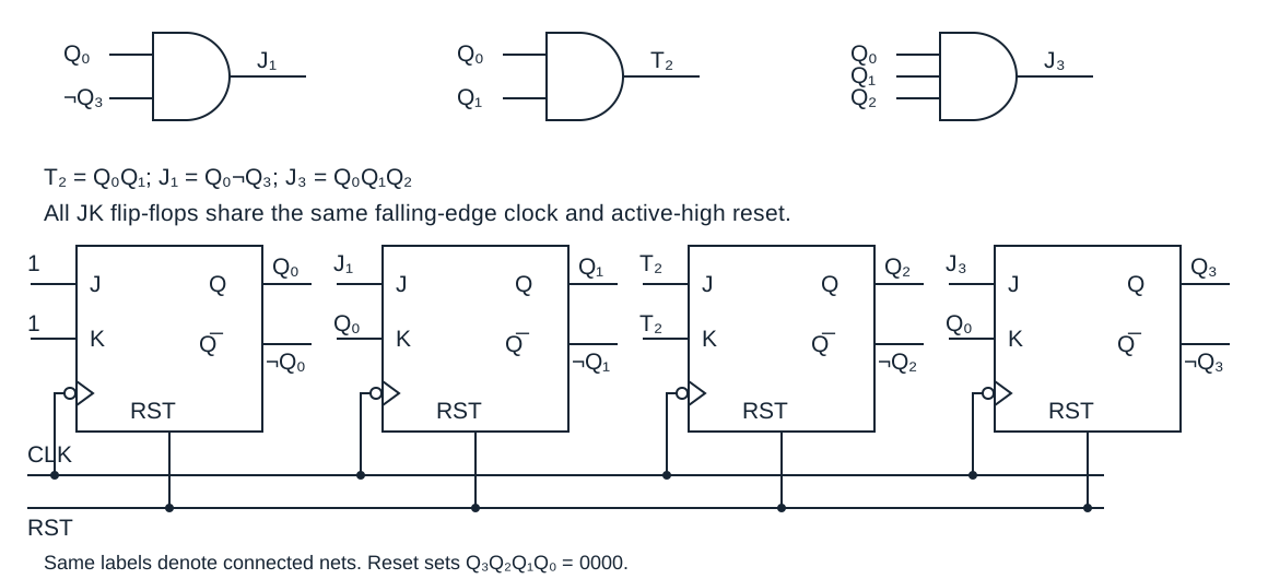
Use the common falling-edge clock and reset of (2). The required JK inputs are
With , these connections produce the ten transitions in (3).
(5)
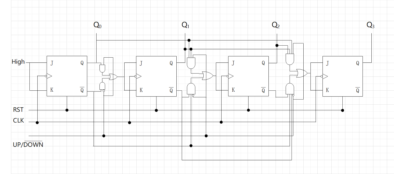
Writing , the toggle inputs in (5) are
Thus counts up modulo 16, while counts down modulo 16.