東京大学 情報理工学系研究科 コンピュータ科学専攻 2021年2月実施 問題2
Author
zephyr, 祭音Myyura
Description
Answer the following questions on digital circuits.
(1) Design and depict a circuit equivalent to XOR (exclusive OR) gate by using at most five 2-input NAND gates.
(2) Design and depict a 1-bit full-adder by using only two 2-input XOR gates and three 2-input NAND gates.
(3) Design and depict a 4-bit adder circuit by using four 1-bit full-adders. You may use 2-input NAND gates, 2-input NOR gates, and NOT gates, if necessary. Indicate also the critical path of the 4-bit adder circuit.
(4) Consider a 4-bit clock-synchronous up-down binary counter circuit. The circuit has a 1-bit input CLK for the clocking. The circuit also has a 1-bit input X and a 4-bit output Y. The circuit counts a number from 0 to 15, and outputs the counter value to the output Y. When the input X is '1', the counter value is incremented by one for each positive clock edge. Otherwise, the counter value is decremented by one for each positive clock edge. The circuit allows overflows, i.e. the next counter value is 0 when the current counter value is 15 and the input X is '1', and the next counter value is 15 when the current counter value is 0 and the input X is '0'. Assume that the circuit satisfies the setup-time and hold-time constraints. Design and depict the 4-bit clock-synchronous up-down binary counter circuit. You may use 1-bit full-adders, D-flip-flops, 2-input NAND gates, 2-input NOR gates, and NOT gates, if necessary.
回答以下关于数字电路的问题。
(1) 设计并描绘一个等效于 XOR(异或)门的电路,最多使用五个 2 输入 NAND 门。
(2) 设计并描绘一个 1 位全加器,仅使用两个 2 输入 XOR 门和三个 2 输入 NAND 门。
(3) 设计并描绘一个 4 位加法器电路,使用四个 1 位全加器。可以使用 2 输入 NAND 门、2 输入 NOR 门和 NOT 门(如有必要)。同时标明 4 位加法器电路的关键路径。
(4) 考虑一个 4 位时钟同步上下计数二进制计数器电路。电路有一个用于时钟的 1 位输入 CLK。电路还有一个 1 位输入 X 和一个 4 位输出 Y。电路计数从 0 到 15,并将计数值输出到输出 Y。当输入 X 为 '1' 时,计数值在每个正时钟边沿递增 1。否则,计数值在每个正时钟边沿递减 1。电路允许溢出,即当当前计数值为 15 且输入 X 为 '1' 时,下一个计数值为 0,当当前计数值为 0 且输入 X 为 '0' 时,下一个计数值为 15。假设电路满足设置时间和保持时间约束。设计并描绘这个 4 位时钟同步上下计数二进制计数器电路。可以使用 1 位全加器、D 触发器、2 输入 NAND 门、2 输入 NOR 门和 NOT 门(如有必要)。
题目描述
回答下列数字电路问题。
(1)仅用至多五个二输入 NAND 门,设计并画出等价于异或门的电路。
(2)仅用两个二输入 XOR 门和三个二输入 NAND 门,设计并画出一位全加器。
(3)用四个一位全加器设计并画出四位加法器;必要时可使用二输入 NAND 门、二输入 NOR 门和非门,并标明该四位加法器的关键路径。
(4)设计并画出四位时钟同步二进制加减计数器。电路有一位时钟输入
CLK、一位控制输入 X 和四位输出 Y,计数范围为 至 :
每个时钟上升沿,当 X=1 时加一,否则减一;允许模 溢出,即
加一变为 , 减一变为 。假定满足建立时间与保持时间约束。
必要时可使用一位全加器、D 触发器、二输入 NAND/NOR 门及非门。
Kai
(1)
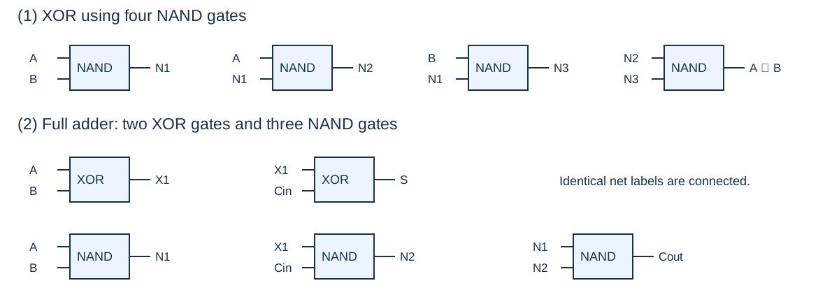
The XOR gate can be constructed using four NAND gates as follows:
Steps:
The circuit can be depicted as:
A ----+--------[N2]----\
     |          ^       \
     +--[N1]----+        [N4]---- XOR
     |          v       /
B ----+--------[N3]----/
(2)
A 1-bit full-adder has three inputs: , , and , and two outputs: (sum) and (carry out).
Using XOR and NAND gates:
- which is
- which is
- which is
- which is
- which is
(3)
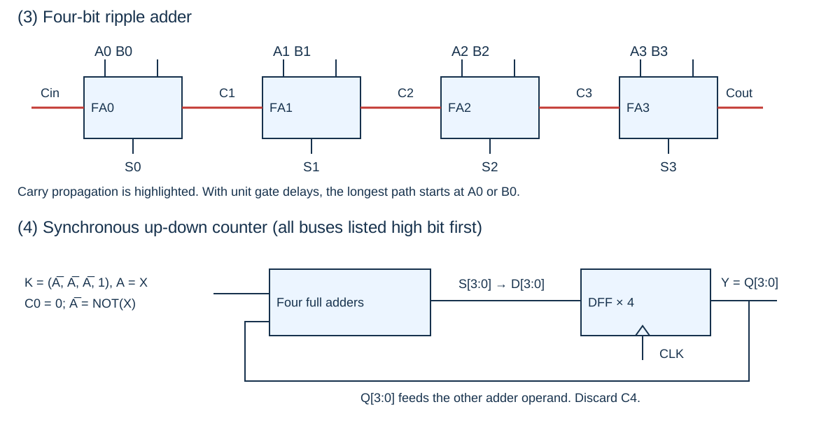
A 4-bit adder can be created by chaining four 1-bit full-adders. The carry-out from each adder becomes the carry-in for the next adder.
For each 1-bit full-adder:
- Inputs: , ,
- Outputs: ,
The critical path is the longest delay path through the adders, which goes through all carry-out to carry-in connections.
(A0,B0,Cin) -> FA0 -> S0,C1
(A1,B1,C1)  -> FA1 -> S1,C2
(A2,B2,C2)  -> FA2 -> S2,C3
(A3,B3,C3)  -> FA3 -> S3,Cout
The carry chain traverses all four full-adders. Using the gates in (2), let be the delays of one XOR and one NAND gate. The longest paths to and have delays and , respectively; the critical delay is their maximum. If every gate has unit delay, the critical path starts at or , passes through the first XOR, and then through the eight NAND gates on the carry chain to , for a delay of nine. The path from alone has only eight gate delays.
(4)
令 为第 个 D 触发器当前保存的位, 和 分别为第 个全加器的和与进位输出。四个 D 触发器共用 CLK,且
四个全加器组成行波加法器,计算
令最低位加法器的进位输入 ,第 位的输入为
每个全加器满足
连接 ()。各 接相应 D 触发器的 D 输入,Q 输出既构成 ,也反馈到加法器;最高位进位丢弃。
Q[3:0] ----\
             4-bit ripple adder ---- S[3:0] ---- DFF[3:0] ---- Y=Q[3:0]
K[3:0] ----/          (C0=0)                         ^
                                                    CLK
是模 下的 ,故上升沿时 得到 , 得到 ,溢出也自动满足题意。
Knowledge
逻辑电路 布尔代数 加法器 D触发器
解题技巧和信息
- 使用 NAND 门实现基本逻辑功能
- 将全加器串联实现多位加法器
- 设计同步计数器时注意正负边缘触发逻辑
重点词汇
- exclusive OR 异或
- full-adder 全加器
- counter 计数器
- clock-synchronous 时钟同步
- up-down binary counter 二进制上下计数器
参考资料
- Digital Design and Computer Architecture by David Harris and Sarah Harris - Chap. 3, 5
- Fundamentals of Digital Logic with VHDL Design by Stephen Brown and Zvonko Vranesic - Chap. 4