東京大学 情報理工学系研究科 コンピュータ科学専攻 2020年8月実施 専門科目 問題3
Author
zephyr, 祭音Myyura
Description
Consider bit-serial communication circuits which send and receive 5-bit information bit-by-bit in a noisy environment. The 5-bit information consists of a 2-bit start-bit signal, 2-bit payload data, and a 1-bit odd-parity signal.
The sender circuit always outputs '0' in the initial state. At the beginning of a communication, the sender outputs 2-bit data '11' bit-by-bit. It subsequently outputs 2-bit payload data bit-by-bit from the most significant bit. It finally outputs an odd-parity signal such that the number of '1's in the sent bit sequence including the 2-bit start-bit signal, the payload data, and the parity signal itself is an odd number. After sending the parity signal, the sender circuit goes to the initial state, and it outputs '0' until the next sending.
The receiver circuit has a 1-bit input A from the sender circuit, a 1-bit output B for the parity check result, and a 2-bit output for the received payload data. It obtains payload data from a received bit sequence and does the odd parity checking.
In the initial state, the receiver circuit waits for '1' corresponding to the first bit of a start-bit signal. In the next clock cycle after receiving the first bit of a start-bit signal, it receives a value corresponding to the second bit of a start-bit signal. If the received value corresponding to the second bit of a start-bit signal is '0', the receiver circuit judges that the first received bit '1' was an error caused by a noise, and goes back to the initial state. Otherwise, in the next 2 clock cycles, it stores each value of the input A as payload data. At the next clock cycle, it receives a parity-bit, and it verifies that the number of '1's in the received 5-bit sequence consisting of the 2-bit start-bit signal, the 2-bit payload data, and the parity-bit is odd. It assigns '1' to the output B if the number of '1's is odd, and it assigns '0' otherwise. The value of the output B is always '0', except in the clock cycles for receiving a parity-bit. The receiver circuit then goes to the initial state, regardless of the parity-check result.
Answer the following questions.
(1) Give the state transition diagram of a Mealy-type finite state machine (FSM), consisting of 7 states, for the parity check circuit with the input A and the output B in the receiver circuit. Based on the state transition diagram, give also a corresponding state transition table and an output table by using the one-hot encoding. One-hot encoding is a method for encoding each state as a bit sequence where only one bit is '1' and the other bits are '0'.
(2) Based on the state transition table and the output table in question (1), express the output B as a Boolean expression in terms of the input A and the one-hot encoding representation of the current state of the FSM. Based on the Boolean expression, give also a corresponding gate-level circuit of the parity check circuit that outputs B, given A and the one-hot encoding representation of the current state of the FSM as inputs. You are allowed to use only 2-input AND gates, 2-input OR-gates, and NOT-gates. There is no limitation on the number of gates. You need not describe unused input signals.
(3) According to the Boolean expression answered in question (2), give a CMOS transistor level circuit that outputs B, given A and the one-hot encoding representation of the current state of the FSM as inputs. You are not allowed to use more than 12 transistors. You may use the inverter mark, but the number of transistors required for the inverters must be included in the total number of transistors. You need not describe unused input signals.
题目描述
考虑在有噪环境中逐位收发五位信息的串行通信电路。五位依次为两位起始信号、两位有效载荷和一位奇校验位。发送器初始状态始终输出 0;开始发送时先逐位输出 11,再从最高位开始输出两位载荷,最后输出校验位,使包含起始位、载荷和校验位在内的五位中 1 的总数为奇数;随后回到初始状态并保持输出 0。
接收器有来自发送器的一位输入 、表示校验结果的一位输出 和两位载荷输出。初始时等待起始信号的第一个 1;下一拍若第二个起始位为 0,则把首个 1 视为噪声并回到初始状态,否则在随后两拍存储载荷,再下一拍接收校验位并检查五位中 1 的个数是否为奇数:奇数时令 ,否则为 。除接收校验位的时钟周期外 始终为 ;校验后无论结果如何均回到初始状态。
(1)给出具有 个状态、输入为 、输出为 的 Mealy 型奇校验 FSM 状态转移图;再采用 one-hot 编码给出相应状态转移表和输出表。one-hot 编码中每个状态由仅一位为 1 的位串表示。
(2)根据第(1)问的表,用输入 和当前状态的 one-hot 表示写出输出 的布尔表达式,并画出相应门级电路。只允许二输入与门、二输入或门和非门,门数不限,未使用的输入信号无需描述。
(3)依据第(2)问的表达式,画出以 和当前 one-hot 状态为输入、输出 的 CMOS 晶体管级电路。最多使用 个晶体管;可用反相器符号,但反相器所需晶体管也计入总数,未使用的输入无需描述。
Kai
(1)
State Transition Diagram
Use the following seven states.
- S0: Initial state, waiting for the first start bit. If '0' is received, return to the initial state. If the first start bit '1' is received, move to the next state.
- S1: Received the first start bit '1'; waiting for the second start bit.
- S2: Received the second start bit '1'; waiting for the first payload bit.
- S3, S4: Received the first payload bit; the running parity is even/odd, respectively.
- S5, S6: Received both payload bits; the running parity is even/odd, respectively. The next bit is the parity bit, after which the FSM returns to S0.
State transitions and outputs B based on input A are as follows (A/B means input/output):
The corresponding state transition and output tables are as follows:
| State | S0 | S1 | S2 | S3 | S4 | S5 | S6 |
|---|---|---|---|---|---|---|---|
| Next State | S0 | S0 | S3 | S5 | S6 | S0 | S0 |
| Output B | 0 | 0 | 0 | 0 | 0 | 0 | 1 |
| Next State | S1 | S2 | S4 | S6 | S5 | S0 | S0 |
| Output B | 0 | 0 | 0 | 0 | 0 | 1 | 0 |
(2)
Use the following seven-bit one-hot encoding:
- S0: 1000000
- S1: 0100000
- S2: 0010000
- S3: 0001000
- S4: 0000100
- S5: 0000010
- S6: 0000001
The output B will be '1' only in states S5 and S6. So the output B can be expressed as a Boolean function of the current state and input A:
Gate-Level Circuit: We can construct the circuit using 2-input AND gates, OR gates, and NOT gates.
- The circuit for :
The circuit for can be implemented using the following logic gates:
S6 -------------\
               AND----\
  /-----NOT-----/      \
 /                      \
A                        OR----> B
 \                      /
  \-------------\      /
               AND----/
S5 -------------/
(3)
The expression is a 2-to-1 multiplexer. Generate with one CMOS inverter and use two CMOS transmission gates:
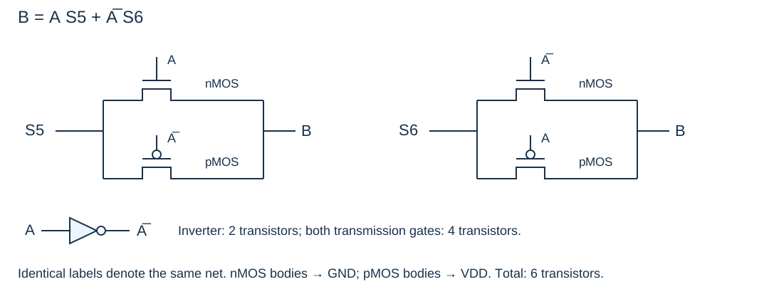
Exactly one transmission gate is on: is passed when , and is passed when . Each transmission gate uses one nMOS and one pMOS, and the inverter uses two transistors, for a total of transistors.
Knowledge
有限状态机 梅利型FSM 一热编码 布尔代数 逻辑电路 CMOS电路
难点解题思路
- 确保正确理解有限状态机的工作流程。
- 确保状态转移图正确,涵盖所有状态和过渡条件。
- 在布尔表达式的转换中,小心处理所有状态编码及其转换关系。
解题技巧和信息
- 在设计状态机时,使用一热编码可以简化状态转换逻辑。
- 对于布尔表达式,尝试先使用基本的逻辑门,再优化以满足设计约束。
- CMOS 电路设计中的每个逻辑门都需要考虑所使用的晶体管数量,确保优化。
重点词汇
finite state machine 有限状态机
Mealy-type FSM 梅利型有限状态机
one-hot encoding 一热编码
parity check 奇偶校验
boolean expression 布尔表达式
参考资料
- "Digital Design and Computer Architecture" by David Harris, Sarah Harris, Chap. 3
- "CMOS VLSI Design: A Circuits and Systems Perspective" by Neil Weste, David Harris, Chap. 4