東京大学 情報理工学系研究科 コンピュータ科学専攻 2017年2月実施 専門科目 問題4
Author
Codex
Description
Independent problem summary (English)
Official examination paper, Problem 4
Design a binary recurrence generator using AND, OR, NOT gates and positive-edge-triggered D flip-flops. Gates have negligible delay; the ideal clock has no skew and connects only to flip-flop clock inputs. For positive integers , initial bits determine
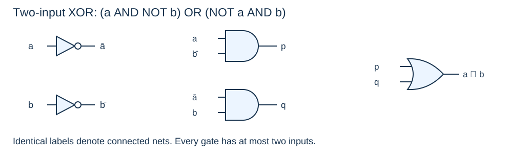
(1) Construct a two-input XOR circuit from the permitted gates.
(2) Three flip-flops are cascaded: the external input feeds , feeds , and feeds . They share the clock and initially store zero. Draw all three outputs for the input and clock below.
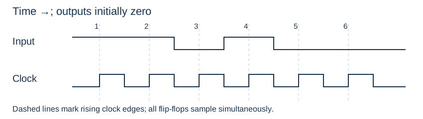
(3) Use 512 flip-flops, and . Initially and exactly at the selected tap indices. Design the circuit so that after clock edges, .
(4) Add inputs . When , each rising edge must copy into and into . When , perform the recurrence from (3). Give the required circuit changes.
Kai
(1)
For two input bits ,
Use two NOT gates, two AND gates and one OR gate. The two AND outputs are disjoint: the result is one precisely for or .
(2)
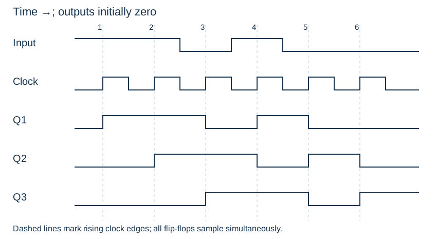
At every rising edge, all flip-flops sample their inputs simultaneously. If is the external input at the -th edge, then
All three outputs retain their values between rising edges. With the given initial zeros:
| Rising edge | 1 | 2 | 3 | 4 | 5 | 6 |
|---|---|---|---|---|---|---|
| Input | 1 | 1 | 0 | 1 | 0 | 0 |
| 1 | 1 | 0 | 1 | 0 | 0 | |
| 0 | 1 | 1 | 0 | 1 | 0 | |
| 0 | 0 | 1 | 1 | 0 | 1 |
(3)
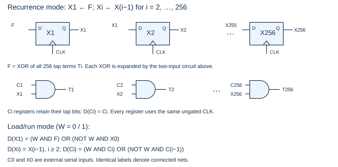
Let and also denote the current output bits of their flip-flops. Form the combinational feedback
A cascade or tree of 255 two-input XOR circuits from (1) implements this expression; each tap term requires an AND gate. Connect the D inputs as follows:
All 512 flip-flops share the unchanged clock. Each retains its initialized tap bit.
To prove correctness, suppose that after edges, . Immediately before edge ,
Thus the next value of is , and for the next value is
The initialization supplies the induction base .
(4)
A multiplexer selecting when and when can be implemented as
Use it at the D inputs:
Here are external inputs. For , both modes require the same shift of , so no selection gate is needed there. The tap registers shift in load mode and retain their values in recurrence mode. The clock continues to connect only to the flip-flop clock pins.
To load prescribed values , keep for 256 rising edges and supply at edge . After the final load edge, all registers contain their prescribed values; set to begin generation.