東京大学 情報理工学系研究科 創造情報学専攻 2019年8月実施 筆記試験 第2問
Author
tomfluff, itsuitsuki, 祭音Myyura
Description
原題
Consider making a memory that can be accessed randomly, using D-FFs (Flip Flop) and 2:1 multiplexers.
Assume that the D-FF is a circuit that stores 1 bit as shown in Fig. 1. A 1-bit signal given to d is written to this circuit at the rise of the clock signal clk, and this circuit continues to output the written signal to q.
As shown in Fig. 2, the 2:1 multiplexer is a circuit that selects one of the two input signals a and b according to the selection signal s and outputs it to c.
(1) Give a truth table for the 2:1 multiplexer shown in Fig. 2. Assume that this multiplexer selects a when s is and selects b when s is .
(2) Draw a circuit diagram of a memory that stores 4 bits and outputs 1 bit at the position specified by a 2-bit address according to the following instructions:
- Use only two kinds of components, which are the D-FF shown in Fig. 1 and the 2:1 multiplexer in Fig. 2.
- Ignore circuits related to clock and write (do not connect anything to
clkandd). - Specify the address of data stored in each D-FF in the circuit diagram.
- Specify the lower bit of the 2-bit address signal wires as
addr_lowand the upper bit of it asaddr_highin the circuit diagram. - Specify the output wire of the memory as
outputin the circuit diagram.
(3) In the similar way as in (2), consider a memory that stores bits and outputs 1 bit at the position specified by an n-bit address using the D-FF shown in Fig. 1 and the 2:1 multiplexer shown in Fig. 2. Give how many multiplexers you need to make this memory.
(4) The D-FF shown in Fig. 3 is a D-FF with write control. In this D-FF, the signal given to d is written only when the input to the write enable signal we is at the rise of the clock signal clk.
If we is , a previously written signal continues to be output to q without updating the stored contents.
Give a circuit diagram of this D-FF in Fig. 3 using only the D-FF in Fig. 1 and the 2:1 multiplexer in Fig. 2. Assume that this multiplexer selects a when s is and selects b when s is .
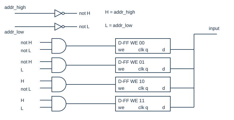
(5) Draw a circuit diagram of a memory that stores 4 bits according to the following instructions:
- Assume that, at the rise of the clock signal, 1 bit data is written at the position specified by a 2-bit address.
- Use only three kinds of components, which are the D-FF with write control shown in Fig. 3, the AND gate shown in Fig. 4, and the NOT gate shown in Fig. 5.
- You can use up to four AND gates and up to two NOT gates.
- Ignore circuits related to clock output (do not connect anything to
clkandq). - Specify the address of data stored in each D-FF in the circuit diagram.
- Specify the lower bit of the 2-bit address signal wires as
addr_lowand the upper bit of it asaddr_highin the circuit diagram. - Specify the data input wire of the memory as
inputin the circuit diagram.

题目描述
使用 D 触发器(D-FF)和 2:1 多路选择器制作可随机访问的存储器。图 1 的 D-FF 存 1 位:在时钟 clk 上升沿把输入 d 写入,随后从 q 持续输出。图 2 的 2:1 多路选择器根据选择信号 s 从输入 a,b 中选一个输出到 c。
- 写图 2 多路选择器真值表:
s=0选a,s=1选b。 - 只用图 1 D-FF 和图 2 多路选择器,画一个存 4 位、由 2 位地址选择并输出其中 1 位的电路。忽略时钟与写入电路,不连接
clk,d;标明每个 D-FF 所存数据的地址;把地址低、高位线分别标为addr_low、addr_high,存储器输出线标为output。 - 类似地,用上述元件制作存 位、由 位地址选 1 位输出的存储器,求所需多路选择器数量。
- 图 3 是带写使能的 D-FF:只有
clk上升沿时we=1才把d写入;we=0时保持原内容并继续从q输出。只用图 1 普通 D-FF 和图 2 多路选择器实现图 3,画电路;多路选择器仍为s=0选a、s=1选b。 - 按以下要求画存 4 位的写入电路:在时钟上升沿,把 1 位输入写到 2 位地址指定位置;只用图 3 带写控 D-FF、图 4 AND 门、图 5 NOT 门;AND 最多 4 个,NOT 最多 2 个;忽略时钟和读出,不连接
clk,q;标明每个 D-FF 地址;地址线标addr_low、addr_high,数据输入线标input。
Kai
(1)
| a | b | s | MUX |
|---|---|---|---|
| 0 | 0 | 0 | 0 |
| 0 | 0 | 1 | 0 |
| 0 | 1 | 0 | 0 |
| 0 | 1 | 1 | 1 |
| 1 | 0 | 0 | 1 |
| 1 | 0 | 1 | 0 |
| 1 | 1 | 0 | 1 |
| 1 | 1 | 1 | 1 |
(2)
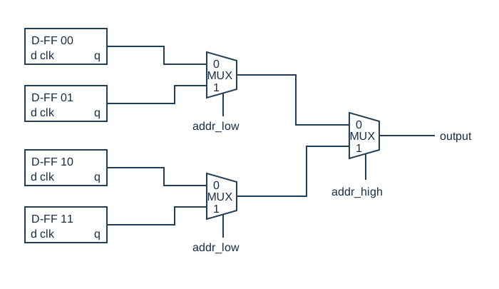
The two first-stage selectors use addr_low, and the final selector uses addr_high. The d and clk terminals remain unconnected.
(3)
Given the circumstances, we would need:
Since we gradually divide all inputs into 2 as inputs to the MUX, so the first layer would be the second and so on, until we have as the final MUX which would give the correct output.
(4)
Connect the D-FF output q to multiplexer input a, the external input d to input b, and we to the selector. The multiplexer output feeds the D-FF data input; the external clock feeds its clock input.
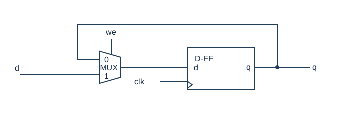
At a rising clock edge, ; between edges, remains unchanged.
(5)
Let and . Use two NOT gates to share , then four AND gates to generate
All four d inputs receive input; only the selected D-FF has write enable 1. Identically named wires in the diagram are the same signal. The clk and q terminals remain unconnected as requested.