東京大学 情報理工学系研究科 創造情報学専攻 2015年8月実施 筆記試験 第1問
Author
Description
日本語
電子部品を使い、進1桁のカウンタを作ろう。ここでは2以上の整数とする。このカウンタはクロック信号 (CLK信号) とイネーブル信号 (EN信号) を入力とし、カウンタ値を出力する (図1)。CLK信号およびEN信号はHとLの2値をとる。CLK信号は図2に示すような周期的信号であり、LからHへの変化をCLK信号の立ち上がりと呼ぶ。カウンタ値はで、起動時にに初期化される。
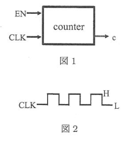
例として2進1桁カウンタを考えよう。このカウンタはCLK信号の立ち上がりの前のカウンタ値を、立ち上がり後のカウンタ値をとすると、CLK信号の立ち上がり時に
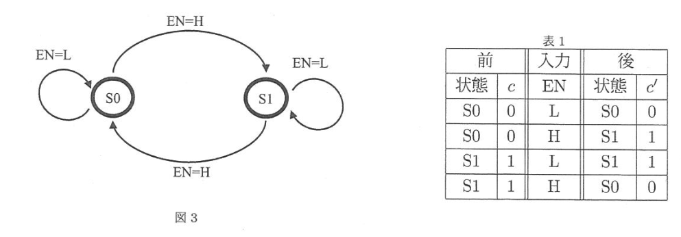
となる。ここで演算子は正の剰余を返す。この2進1桁のカウンタの状態遷移図の例を図3に、状態遷移表の例を表1に示す。ここでS0, S1はそれぞれカウンタ値を0,1とする状態とする。
以下の設問に答えよ。
(1) CLK信号の立ち上がり時に
となるような3進1桁カウンタの状態遷移図および状態遷移表を示せ。状態遷移図と状態遷移表は例と異なるフォーマットを用いてもかまわない。
(2) 設問(1)のカウンタをアップダウンカウンタに拡張しよう。EN信号の代わりにアップダウン信号 (UD信号) を入力とし、CLK信号の立ち上がり時に
となる3進1桁アップダウンカウンタの状態遷移図および状態遷移表を示せ。状態遷移図と状態遷移表は例と異なるフォーマットを用いてもかまわない。
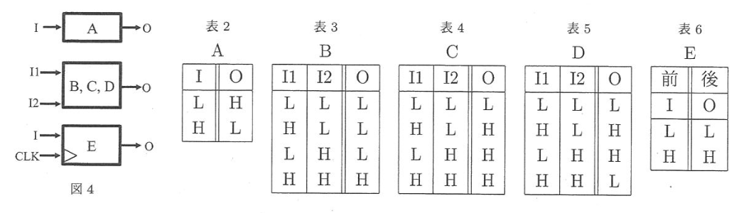
以下の部品を組み合わせ、設問(1)と設問(2)で示したカウンターを実現しよう。部品A, B, C, D, Eの入力、出力を図4に示す。入力値と出力値の関係をそれぞれ表2, 3, 4, 5, 6に記す。部品Eでは、CLK信号の立ち上がり直前の入力Iの値が、立ち上がり後出力Oに設定される。一般に部品A, B, C, D, Eは、それぞれNOT, AND, OR, XOR, D-フリップフロップと呼ばれる。
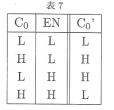
EN信号、カウンタ値はCLK信号の立ち上がりで変化するとする。まず2進1桁のカウンタの例を示す。2進カウンタ値は0か1なので、を2値信号である信号で表現し、信号は、ならL、ならHとする。CLK信号の立ち上がり前の信号を、立ち上がり後の信号をとすると、との関係は表7となり、この2進1桁のカウンタは、例えば、図5に示す回路図で実現される。

以下の設問に答えよ。ただし、全ての部品は十分あり、また全種類を使う必要はない。
(3) 設問(1)で示した3進1桁カウンタを実現するように部品を組み合わせ、回路図を示せ。ここでカウンタ値は2bitで表現すること。通常の論理回路図を描いても良い。
(4) 設問(2)で示した3進1桁アップダウンカウンタを実現するように部品を組み合わせ、回路図を示せ。ここでカウンタ値は2bitで表現すること。通常の論理回路図を描いても良い。

(5) 図6に示すように3進1桁カウンタを組み合わせ、3進3桁のカウンタを実現したい。設問(3)で示した3進1桁のカウンタに新たな出力信号を追加する拡張を行うことで、3進3桁カウンタの部品となるような3進1桁のカウンタを実現し、この3進1桁のカウンタを図示せよ。通常の論理回路図を描いても良い。
English (AI translated)
Let's make a base- 1-digit counter using electronic components. Here, let be an integer of 2 or more. This counter takes a clock signal (CLK signal) and an enable signal (EN signal) as inputs and outputs a counter value (Figure 1). The CLK signal and EN signal take two values, H and L. The CLK signal is a periodic signal as shown in Figure 2, and the change from L to H is called the rising edge of the CLK signal. The counter value is and is initialized to at startup.
As an example, let's consider a base-2 1-digit counter. Let be the counter value before the rising edge of the CLK signal, and be the counter value after the rising edge. At the rising edge of the CLK signal:
Here, the operator returns a positive remainder. An example of the state transition diagram for this base-2 1-digit counter is shown in Figure 3, and an example of the state transition table is shown in Table 1. Here, S0 and S1 are states where the counter value is 0 and 1, respectively.
Answer the following questions.
(1) Show the state transition diagram and state transition table for a base-3 1-digit counter such that at the rising edge of the CLK signal:
You may use a format different from the example for the state transition diagram and state transition table.
(2) Let's extend the counter in question (1) to an up-down counter. Taking an up-down signal (UD signal) as input instead of the EN signal, show the state transition diagram and state transition table for a base-3 1-digit up-down counter such that at the rising edge of the CLK signal:
You may use a format different from the example for the state transition diagram and state transition table.
Let's realize the counters shown in questions (1) and (2) by combining the following components. The inputs and outputs of components A, B, C, D, and E are shown in Figure 4. The relationships between input values and output values are described in Tables 2, 3, 4, 5, and 6, respectively. In component E, the value of input I immediately before the rising edge of the CLK signal is set to output O after the rising edge. Generally, components A, B, C, D, and E are called NOT, AND, OR, XOR, and D-Flip-Flop, respectively.
Assume that the EN signal and the counter value change at the rising edge of the CLK signal. First, an example of a base-2 1-digit counter is shown. Since the base-2 counter value is 0 or 1, is represented by a binary signal signal, where the signal is L if and H if . If the signal before the rising edge of the CLK signal is and the signal after the rising edge is , the relationship between and is as shown in Table 7. This base-2 1-digit counter is realized, for example, by the circuit diagram shown in Figure 5.
Answer the following questions. Note that there are enough of all components, and it is not necessary to use all types.
(3) Combine the components to realize the base-3 1-digit counter shown in question (1) and show the circuit diagram. Here, the counter value should be represented by 2 bits. You may draw a standard logic circuit diagram.
(4) Combine the components to realize the base-3 1-digit up-down counter shown in question (2) and show the circuit diagram. Here, the counter value should be represented by 2 bits. You may draw a standard logic circuit diagram.
(5) As shown in Figure 6, we want to combine base-3 1-digit counters to realize a base-3 3-digit counter. Realize a base-3 1-digit counter that serves as a component for the base-3 3-digit counter by extending the base-3 1-digit counter shown in question (3) to add a new output signal, and illustrate this base-3 1-digit counter. You may draw a standard logic circuit diagram.