東京大学 情報理工学系研究科 創造情報学専攻 2012年8月実施 筆記試験 第2問
Author
Description
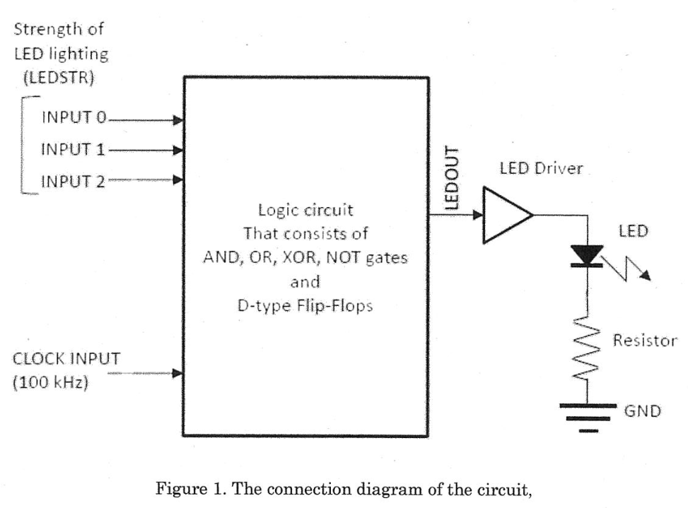
Official examination, archived Japanese PDF. Design a logic circuit to light an LED satisfying the following conditions. Figure 1 shows the connection diagram of the circuit, input signals and an output signal to the LED.
Condition 1: Inputs of the circuit to design are LEDSTR and CLOCK INPUT ( clock input signal). The output of the circuit to design is LEDOUT. LEDOUT is directly connected to the LED driver and lights the LED. When LEDOUT is H, LED is on, and when LEDOUT is L, LED is off.
Condition 2: LEDSTR (INPUT 0, INPUT1, INPUT2) specifies the strength of the LED lighting. When LEDSTR is 0, the LED is completely turned off. When LEDSTR is 5, the LED is continuously turned on. When 1 <= LEDSTR <= 4, the strength of the light from the LED is proportional to the value of LEDSTR. When LEDSTR is more than or equal to 6, any behavior of the circuit is allowed.
Condition 3: When the LED turns on and off repeatedly at more than , the strength of the LED light is seen as an average value of the time periods when the LED is turned on.
Condition 4: The logic circuit is designed using AND, OR, XOR, NOT and D-type Flip-Flops.
Design the circuit following the questions below.
-
Design a 3-bit counter that count from 0 to 4 repeatedly such as
-
Design a circuit that compares two 3-bit numbers.
-
Design a circuit to turn on the LED for 1 clock period when
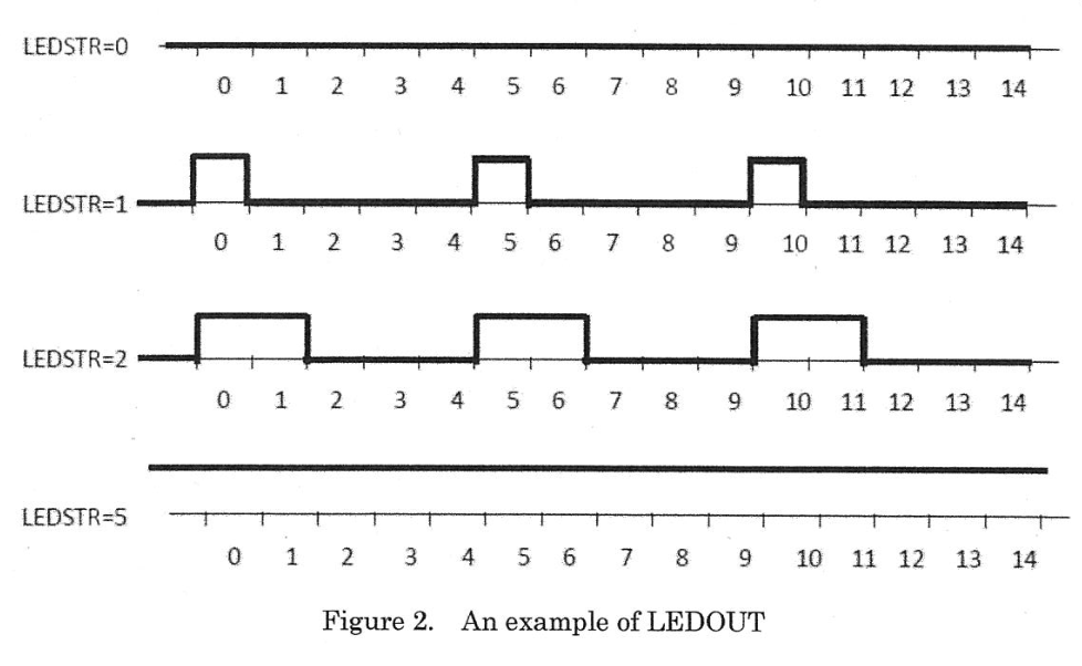
LEDSTRis 1, 2 clock periods whenLEDSTRis 2, ......., 5 clock periods (i.e. always on) whenLEDSTRis 5. Figure 2 is an example of the output waveform. -
Using the logic circuit designed in (3), design a logic circuit that turns the LED on and off with a blinking period longer than one second with the strength of the light specified by
LEDSTR.
题目描述
设计一个控制 LED 亮度的逻辑电路,连接与波形见原文图 1、2,并满足:
- 输入为三位
LEDSTR(INPUT0, INPUT1, INPUT2)和频率 的CLOCK INPUT,输出为直接连接 LED 驱动器的LEDOUT;LEDOUT=H时点亮,LEDOUT=L时熄灭。 LEDSTR指定亮度:为 0 时完全熄灭,为 5 时持续点亮;在 时,感知亮度与其数值成正比;大于等于 6 时电路行为不限。- LED 以高于 的频率反复开关时,人眼感知亮度等于其点亮时间占比对应的平均值。
- 只能使用 AND、OR、XOR、NOT 门和 D 触发器。
按以下步骤设计:
-
设计一个循环计数的 3 位计数器:
-
设计比较两个 3 位数的电路。
-
设计 LED PWM 电路:
LEDSTR为 1 时每 5 个时钟点亮 1 个时钟周期,为 2 时点亮 2 个周期,依此类推;为 5 时点亮 5 个周期,即始终点亮。 -
利用第 3 问电路,再设计一个电路,使 LED 以
LEDSTR指定的亮度点亮一次、熄灭一次,完整的点亮—熄灭周期长于一秒。
Kai
All flip-flops below use the rising edge of the given 100 kHz clock. Let the least significant strength bit be INPUT0, so . AND is written by juxtaposition, OR by , NOT by an overbar, and XOR by .
(1) Modulo-five counter
Use three D flip-flops with outputs . The complete next-state table, including recovery from unused states, is:
| Current | Next |
|---|---|
| 000 | 001 |
| 001 | 010 |
| 010 | 011 |
| 011 | 100 |
| 100 | 000 |
| 101 | 000 |
| 110 | 000 |
| 111 | 000 |
A gate implementation is
Connect each expression to the corresponding D input, and connect the same clock to all three flip-flops. The five valid states cycle as required. An arbitrary unused binary startup state enters 000 on the next edge; a known initial phase would additionally require an initialization mechanism, which the question does not specify.
(2) Three-bit comparator
For unsigned inputs and , put . Then
These equations compare the most significant unequal bit and use only the allowed gates. Exactly one output is high for each pair of inputs.
(3) PWM brightness
Connect the counter value to comparator input , and to input . Use its less-than output:
100 kHz ──> modulo-5 counter ── C ──┐
                                   ├─ unsigned C<S ──> LED driver
LEDSTR ─────────────────────── S ──┘
For one full counter cycle , the output is high for exactly clocks when . Thus the duty cycle is : zero is always off and five is always on. Each clock lasts , so the PWM period is and frequency is .
This assumes remains fixed during a frame. In a physical synchronous implementation, sampling the comparator output in an additional D flip-flop eliminates combinational transition glitches; this delays the waveform by one clock but preserves its duty cycle.
(4) Slow blinking at the specified brightness
Add an 18-bit synchronous binary counter driven by the same 100 kHz clock. Implement its D inputs using allowed gates:
Its top bit is a square-wave enable. Each full high or low interval lasts
so a complete blink period is . Gate the existing PWM:
100 kHz ──> modulo-5 counter ──> C<S ──┐
LEDSTR ──────────────────────────^     AND ──> LED driver
100 kHz ──> 18-bit counter ──> b17 ────┘
During , the brightness is the specified PWM brightness; during , the LED is off. At it remains off, as required. A registered final output can again suppress gate glitches. The intervals above are the full steady-state intervals; without a reset the first visible partial interval depends on the initial counter phase. The 18-bit divider is a convenient choice, not a minimum-size claim.