京都大学 情報学研究科 通信情報システム専攻 2023年8月実施 専門基礎A [A-2]
Author
SUN, 祭音Myyura (assisted by ChatGPT 5.4 Thinking)
Description
Answer all the following questions. Note that operators
(1)
Answer the following questions on the logic function
(a) Give all minimum sum-of-products expressions of
(b) Derive a logic circuit that realizes
(c) Assume logic functions
and
Among all the logic functions
derive a minimum sum-of-products expression of a logic function that has the minimum number of product terms with the minimum number of literals in its minimum sum-of-products form. If there is no logic function
(2)
We design a sequential circuit that decodes the variable-length codes defined in Table 1. This sequential circuit has a 1-bit input
Table 1
| fixed-length code | variable-length code |
|---|---|
| 001 | 0 |
| 010 | 10 |
| 011 | 110 |
| 100 | 1110 |
| 101 | 1111 |
(a) Derive a state transition diagram when we design this sequential circuit as a Moore-type sequential circuit that outputs the fixed-length code in the next cycle after the variable-length code is recognized.
(b) Derive a state transition diagram when we design this sequential circuit as a Mealy-type sequential circuit that outputs the fixed-length code immediately after the variable-length code is recognized.
(c) Regarding the state transition diagram derived in (b), show the state transition table and the output table with the minimum number of states. Explain how you verified that the number of states is minimal.
(d) We implement a sequential circuit corresponding to the state transition table and the output table derived in (c) with the minimum number of D flip-flops. Derive the excitation function(s) of the D flip-flop(s) and the output functions of
Kai
(1)
(a) Minimum sum-of-products expression of
Let
 |  |  |
The minimum sum-of-products expression is
This is the unique minimum SOP form.
(b) Realization using the minimum number of 3-input NAND gates
From part (a),
Using a two-level NAND-NAND implementation with only 3-input NAND gates:
Then
Therefore, the minimum number of 3-input NAND gates is
(c) Minimum SOP expression of
Derive the corresponding K-map for
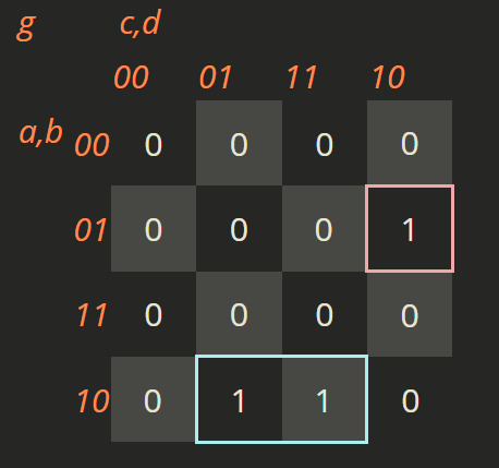 |  | 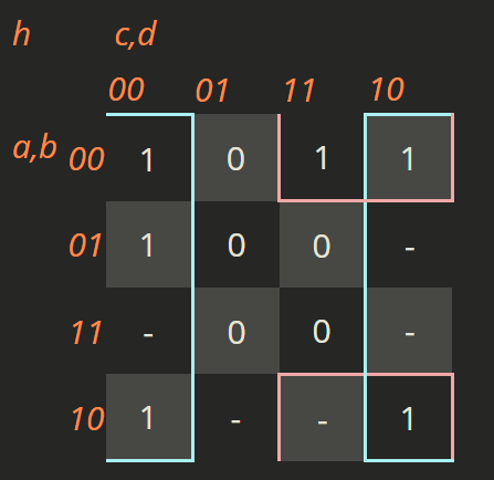 |
We seek
Among all such
(2)
To decode the variable-length codes
we use prefix states corresponding to the partial inputs already seen.
Let:
= initial state (no pending prefix) = prefix 1= prefix 11= prefix 111
(a) Moore-type sequential circuit
State definitions
- S0/000 : initial state
- S1/000 : prefix
1has been read - S11/000 : prefix
11has been read - S111/000 : prefix
111has been read - O001/001 : output state for code
001 - O010/010 : output state for code
010 - O011/011 : output state for code
011 - O100/100 : output state for code
100 - O101/101 : output state for code
101
State transitions
S0/000   --0--> O001/001
S0/000   --1--> S1/000

S1/000   --0--> O010/010
S1/000   --1--> S11/000

S11/000  --0--> O011/011
S11/000  --1--> S111/000

S111/000 --0--> O100/100
S111/000 --1--> O101/101

O001/001 --0--> O001/001
O001/001 --1--> S1/000

O010/010 --0--> O001/001
O010/010 --1--> S1/000

O011/011 --0--> O001/001
O011/011 --1--> S1/000

O100/100 --0--> O001/001
O100/100 --1--> S1/000

O101/101 --0--> O001/001
O101/101 --1--> S1/000

(b) Mealy-type sequential circuit
State definitions
- S0 : initial state
- S1 : prefix
1has been read - S11 : prefix
11has been read - S111 : prefix
111has been read
State transitions with outputs
S0   --0/001--> S0
S0   --1/000--> S1

S1   --0/010--> S0
S1   --1/000--> S11

S11  --0/011--> S0
S11  --1/000--> S111

S111 --0/100--> S0
S111 --1/101--> S0

(c)
Derive the corresponding state transition table:
| Current State | Input | Next State | Output |
|---|---|---|---|
| 00 | 0 | 00 | 001 |
| 00 | 1 | 01 | 000 |
| 01 | 0 | 00 | 010 |
| 01 | 1 | 10 | 000 |
| 10 | 0 | 00 | 011 |
| 10 | 1 | 11 | 000 |
| 11 | 0 | 00 | 100 |
| 11 | 1 | 00 | 101 |
This is already the simplest state transition table. Because all states are distinguishable, meaning no two states produce the exact same output sequence for all possible input sequences
(d)
Derive the corresponding K-map for
 | 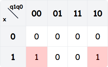 |
 |
In the same way, we have: